Why Do You Have to Simplify Your Most Important Designs Just to Simulate Them?
11.6.2026 | By Manav
Engineering teams are making their most important design decisions on models that have been simplified to fit the simulation tool. Here is why that happens and what changes when the full design is solved at manufacturing resolution.
The designs that carry the most risk are now the hardest to simulate. HBM stacks are moving from 12-high to 16-high within the same height budget. Multi-chiplet packages are passing 1 kW. A full-chip layout can run to hundreds of gigabytes, with billions of polygons and power maps defined at the level of individual functional blocks.
Conventional simulation tools were not built for that level of detail. Engineering teams respond the only way they can: they crop the layout, average the metal density in layers, lump the power map into a handful of regions, and run a few studies they can afford. The result: decisions about warpage, hotspots, and reliability are made on a model that no longer matches the design. That gap delays sign-off, adds margin that costs performance, and pushes problems to the first physical prototype, when they are most expensive to fix.
The Vinci Physics Intelligence Platform now removes that tradeoff. You can spread a single conduction or thermoelasticity simulation, including large displacement, across every GPU in a node, enabling you to solve billions of degrees of freedom on manufacturing-resolution models of the full design. With this new capability, you no longer have to coarsen, homogenize, or crop your largest designs to get an answer.
Why the Largest Designs Get Simplified
A full-chip or full-package study typically follows the same path, and each step removes detail that the design depends on:
The power map is lumped. A design with millions of power-dense blocks is reduced to a few hundred or thousands of averaged regions.
The layers are homogenized. Dense routing, through-silicon vias, and micro-bumps become effective material properties instead of real geometry.
The model is sized to the hardware. The mesh is coarsened until the problem fits in the memory of a single machine.
Only a few variants are run. Each study takes days, so teams test a handful of options and cover the rest with margin.
Each simplification is reasonable on its own. Together, they mean that the hotspot at a block boundary, the warpage concentrated under one HBM stack, or the stress at the edge of a single die can be averaged out of the result. Engineering teams then discover these issues on silicon or in reliability testing, rather than in simulation.
What Physics at Manufacturing Resolution Delivers
Manufacturing resolution means solving the design at the size of its smallest features: every layer, every via, every power-dense block. At that granularity, a model reaches billions of degrees of freedom, beyond what conventional FEA can practically solve within a design cycle. Detail that conventional FEA has to average away is now solved directly, in minutes.
Billions of Degrees of Freedom, Across Every GPU. A single conduction or thermoelasticity simulation now spreads across every GPU in a single node. Users set a GPU count, and Vinci does the rest. Thermoelasticity has reached more than 13 billion DOF on one 8-GPU node in under 8 minutes, and conduction more than 11 billion DOF in under 12 minutes.
Large Displacement at Full Resolution. Thin dies, large substrates, and tall HBM stacks can deflect beyond what a linear model captures. Thermoelasticity with large displacement also runs across multiple GPUs, so engineering teams can predict warpage on the full design without simplifying the stack. In internal tests, we ran 6.6 billion DOF in under 6 minutes on an 8-GPU node.
High-Resolution Parts, Every Detail Included. Every layer, the real geometry, and the full power map stay in one model. We can now support over 1 million individual power sources on a single layer, so each layer can be captured accurately in the model. Hotspots at block boundaries and stress at the edge of a single die stay in the result.
The Workflow in Vinci
Vinci reads the design as it is and solves it on GPUs, without the specialized expertise and manual preparation traditionally required.
Import the full design. Upload the native GDS, OASIS, IPC-2581, or STEP file. Layers, bodies, and hierarchy come with it.
Assign materials. A single configuration file sets the layer stack and materials and works again on the next design revision.
Apply the full power map. Load power sources at the resolution of the design, up to more than 1 million.
Choose the physics and GPU count. Select conduction or thermoelasticity, with large displacement where deflection calls for it, and enter the number of GPUs. Vinci divides the problem among them automatically.
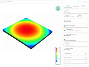
Solve and inspect. Review temperature, displacement, and stress across the whole design, then select any layer or component for its summary values.
All of it runs on standard GPU servers in the customer’s own data center or cloud account, with proprietary design data remaining within their own environment.
Questions You Can Answer on the Full Design
When the full design solves in minutes, engineering teams can ask the questions that cropping and averaging used to hide:
Where does warpage peak across the whole package, and which HBM stack carries the highest stress?
Does a hotspot form at the boundary between two power-dense blocks, once each block carries its own power?
How does a change to the base-die floorplan move junction temperature across the full reticle?
Does the result still hold at full resolution, without homogenized layers?
How far does a thin die or large substrate deflect once displacement is too large for a linear model?
What is the optimal mix of materials, layer thickness, and power sources?
For the first time, engineering teams can simulate their largest designs whole, at manufacturing resolution, without simplifying the model to fit the tool. What once required a homogenized model and a long queue can now run as a single, full-fidelity simulation.
Talk to our team to see your largest, most complex design run in full.
Manav is a product marketing leader with experience at Adobe, Cisco, Samsung, and SpaceX. At Vinci, he leads product marketing for their Physics Intelligence Platform. He holds an MBA from Duke University’s Fuqua School of Business and a B.S. in Computer Science from NC State University.