Deterministic, Solver-Accurate Thermal and Warpage Analysis at Manufacturing Resolution for Advanced 2.5D HBM Packages
Hardik Kabaria, Rahima Mohammed, Satish Radhakrishnan, Vincent Rerolle, Will Stark, Sarah Osentoski, John Bruggeman
April 2026
1. Background
Thermal management has become the defining bottleneck in high-performance computing (HPC) and AI accelerator packaging.
Modern packages integrate high-power ASICs with multiple High Bandwidth Memory (HBM) stacks on a silicon interposer, creating tightly coupled thermal and mechanical interactions. Die-to-die thermal crosstalk elevates HBM junction temperatures, while coefficient of thermal expansion (CTE) mismatch between the epoxy moulding compound, silicon interposer, and organic substrate drives thermo-mechanical warpage that threatens solder joint integrity and long-term reliability.
Each HBM stack now comprises a base die with up to 16 vertically stacked memory dies—compared to four in prior generations—concentrating active silicon in a confined vertical column adjacent to the ASIC. As systems integrate four or more HBM stacks per device, aggregate thermal design power exceeds 1 kW.
At these scales, thermal behavior is governed by fine-grained spatial effects, including tier-level hotspot formation, vertical heat conduction through TSVs, and anisotropic resistance across BEOL layers and micro-bump arrays. Capturing these effects requires simulation at manufacturing resolution.
Conventional finite element analysis (FEA) cannot meet this requirement due to two fundamental limitations:
Computational scale: Package geometries with hundreds of billions of degrees of freedom make high-fidelity FEA impractical for iterative design workflows.
Model fidelity: Standard FEA workflows rely on homogenization, collapsing BEOL layers and micro-bump arrays into isotropic slabs. These approximations remove critical anisotropy and obscure the localized thermal effects that drive HBM reliability risks.
As a result, thermal analysis remains both too slow and too coarse to support modern design cycles.
2. Methodology
This work evaluates Vinci, a system for deterministic, solver-accurate physics computation directly on manufacturing-resolution geometry, using a representative 2.5D package.
The test vehicle comprises two ASICs and eight HBM stacks—four per ASIC—mounted on a silicon interposer and organic substrate. Each HBM stack includes a base die with 16 vertically stacked memory dies, resulting in 136 active die layers and a 692-million degree-of-freedom geometry representative of current and next-generation AI accelerator designs.
The approach addresses the two limitations of conventional FEA—scale and fidelity—through two mechanisms:
Manufacturing-resolution geometry: Vinci operates directly on manufacturing-resolution geometry, resolving BEOL metal layers (nm to µm scale), micro-bump arrays (~15–20 µm pitch), and through-silicon vias (TSVs) at physical dimensions without simplification or manual meshing. Effective thermal conductivity tensors (Keff) are computed per layer via directional solves in X, Y, and Z, preserving anisotropic heat transport. This retains the local thermal resistance and vertical conduction paths that are lost in homogenized models.
Deterministic physics computation: Geometry is ingested from structured configuration data describing layer stackups, material assignments, and component boundaries. The workflow—from geometry ingestion through converged solution—executes without manual intervention.
Thermal boundary conditions are applied as Robin (convective) conditions at maximum thermal design power (TDP) for steady-state analysis, with transient burst profiles used for time-resolved thermal propagation. Thermo-mechanical warpage is computed from CTE mismatch fields derived from the same geometry.
3. Results
The proposed approach enables full-package, manufacturing-resolution analysis across steady-state, transient, and thermo-mechanical domains.
Steady-State Thermal Behavior
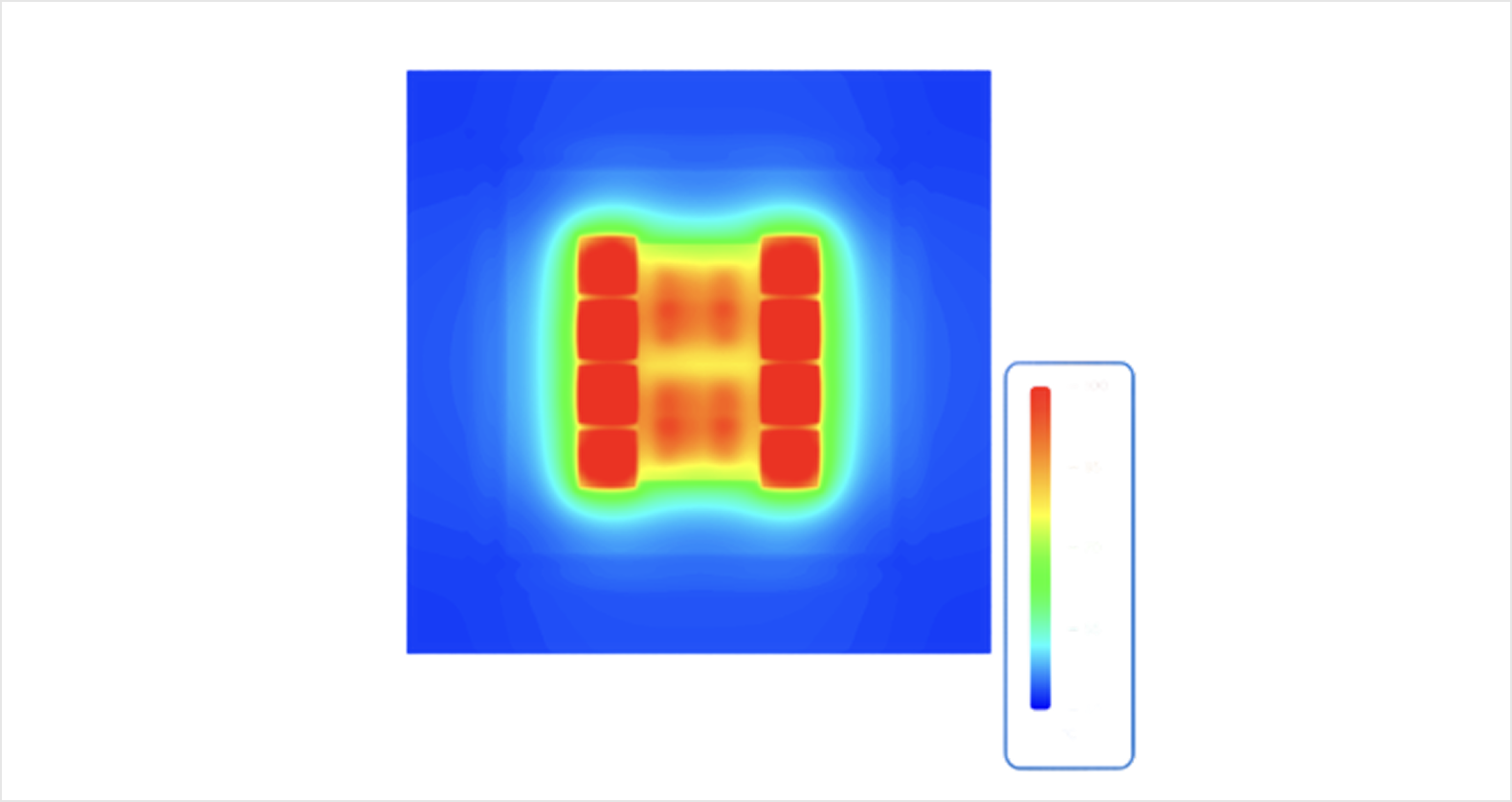
Steady-state hotspot analysis of the 8-HBM, 2-ASIC package at maximum TDP resolves junction temperature at bump-pitch granularity across the full package. The baseline centrally located ASIC configuration produces Tj ≈ 100 °C at the HBM interface (Figure 1), exposing localized BEOL-to-bump thermal crowding that homogenized models do not capture.
Full-resolution temperature maps reveal spatially non-uniform thermal resistance across the interposer, resulting in asymmetric HBM junction temperatures. These effects are directly relevant to thermal-aware floorplanning of the custom HBM base die.
Transient Thermal Response
Transient burst analysis captures thermal wave propagation under high-intensity compute conditions. Results show that short-duration power spikes do not produce transient junction temperature excursions beyond HBM safe-operating-area limits. This behavior cannot be evaluated using steady-state analysis alone and is critical for validating dynamic workload conditions.
Thermo-Mechanical Behavior
Thermo-mechanical warpage is computed from CTE mismatch between the epoxy moulding compound, silicon interposer, and substrate. The results identify package configurations susceptible to solder joint fatigue and delamination, enabling material and geometry tradeoffs prior to fabrication.
Degrees of Freedom
E2E Runtime (Meshing → Convergence) without Keff
E2E Runtime (Meshing → Convergence) with Keff (BEOL + Bumps)
692,692,173
92.65 sec
346 sec
The full package is solved in under six minutes, including manufacturing-resolution Keff computation across all BEOL and bump layers. Equivalent-fidelity FEA typically requires hours to days.
Implication for Design Exploration
This runtime enables systematic design-of-experiments (DOE) studies at manufacturing resolution.
In the full paper, parameterized sweeps are performed across three thermally critical axes:
Power distribution: IP block power variation across the ASIC and HBM base die
Material properties: TIM conductivity and bond-line thickness
Physical configuration: Relative die placement on the interposer
Each configuration produces a full-resolution junction temperature map in seconds, enabling construction of a thermal response surface directly tied to reliability limits across the HBM stack.
This allows identification of operating conditions under which junction temperature remains within specification—and those where it does not—at a level of fidelity and scale not accessible with conventional workflows.
Fig 1: Steady-state temperature map across 8 HBM stacks (4 per ASIC) and 2 ASICs at maximum TDP; Tj ≈ 100 °C at HBM.
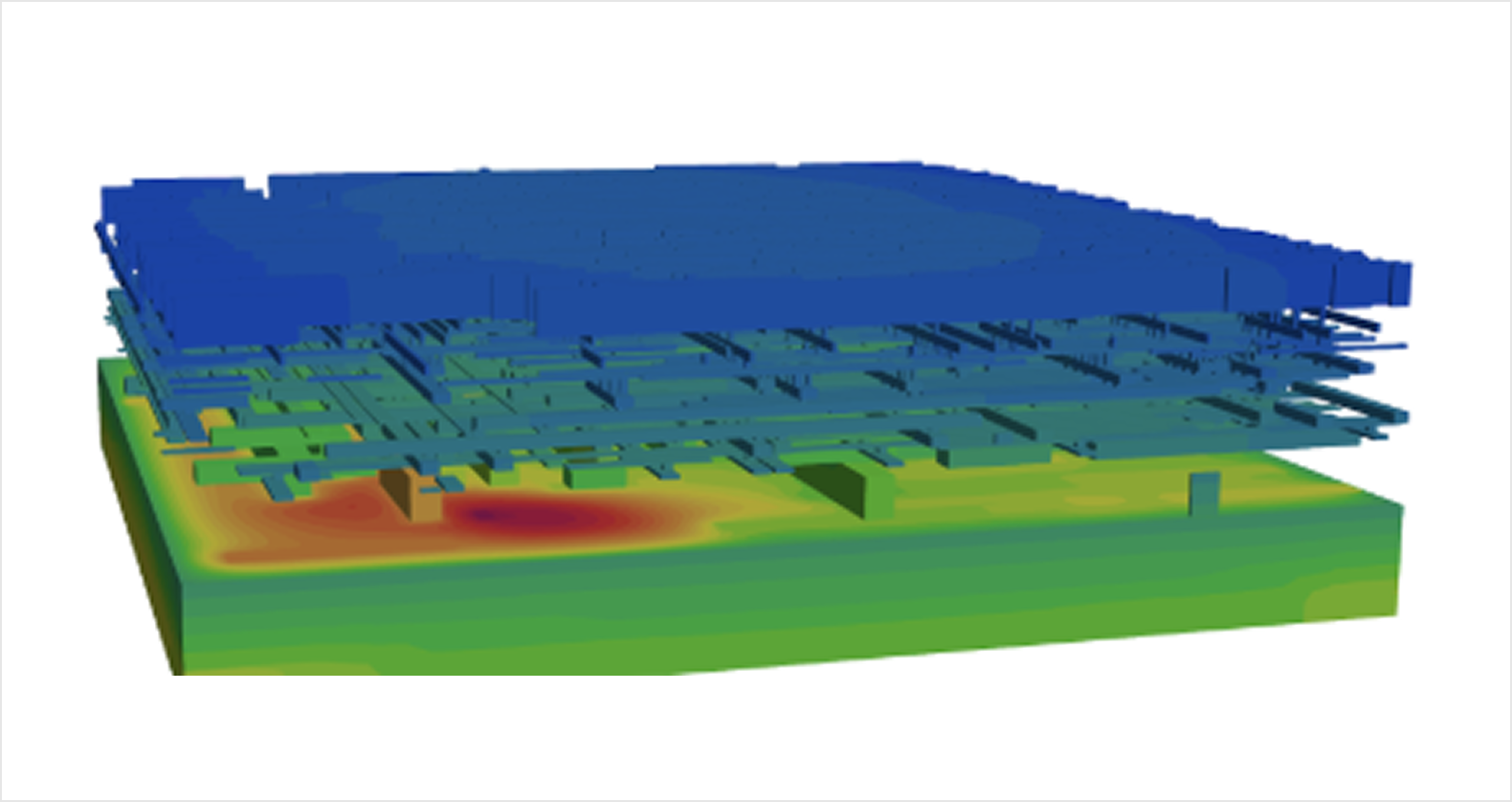
Fig 2: Explicit representation of the multi-layer stackup including BEOL metal layers, micro-bump arrays, and TSVs at manufacturing resolution — no geometry simplification.
4. Conclusions
Combining manufacturing-resolution geometry with deterministic, solver-accurate computation changes the economics of thermal analysis for advanced 2.5D packages.
By resolving BEOL layers, TSVs, and micro-bump structures at physical dimensions—rather than absorbing them into homogenized material properties—the approach exposes failure modes that conventional FEA systematically misses. These include localized thermal crowding at bump pitch, anisotropic heat spreading across the interposer, and transient temperature behavior under burst workloads.
At the same time, end-to-end runtimes on the order of minutes—representing greater than 1000× improvement over conventional workflows—remove simulation as a gating step. Thermal analysis shifts from a late-stage verification activity to a continuously accessible capability within the design process.
This change in speed and fidelity makes systematic exploration of the design space practical. Parameter sweeps across TIM properties, bond-line thickness, die-level power distribution, and placement can be evaluated at full geometric resolution, enabling construction of thermal response surfaces tied directly to reliability limits. Thermal qualification moves from a binary pass/fail check to a continuous, physics-grounded assessment across the operating envelope.
As packaging complexity continues to scale—driven by increased HBM stack height and sub-micron interconnect geometries—the degree-of-freedom requirements exceed what conventional FEA can practically support at full fidelity. A system that operates directly at manufacturing resolution without workflow modification is therefore not only faster, but required to sustain design iteration at these scales.
Authors:
Hardik Kabaria
Founder & Chief Executive Officer, Vinci
Dr. Hardik Kabaria is Founder and Chief Executive Officer of Vinci. His work in computational geometry, physics simulation, and AI underpins the company’s approach to deterministic, solver-accurate systems for engineering and the physical world.
Rahima Mohammed
Semiconductor Technical Advisor, Vinci
Rahima Mohammed is Semiconductor Technical Advisor at Vinci, where she leads strategy for physics-intelligent modeling and AI-accelerated validation in the semiconductor ecosystem. Her work spans multiphysics modeling across thermal, mechanical, and electrical domains, with a focus on advanced cooling, 3DIC packaging, and benchmarking efforts that inform product direction across component, package, and system levels.
Satish Radhakrishnan
Head of GTM - Semiconductor & Electronics, Vinci
Satish Radhakrishnan is Head of GTM - Semiconductor & Electronics at Vinci, where he works at the intersection of technical strategy, industry engagement, and adoption across semiconductor and electronics markets. His background in simulation, packaging, and applied physical systems informs a practical, engineering-led perspective on deploying advanced physics-based tools in production workflows.
Vincent Rerolle
Co-Founder & Chief Commercial Officer, Vinci
Vincent Rerolle is Co-Founder and Chief Commercial Officer at Vinci. He works at the intersection of technical product strategy, industry engagement, and commercialization, helping connect advances in physics-based AI to the practical needs of engineering organizations.
Will Stark
Founding Mechanical Engineer, Vinci
Will Stark is a founding member of the Vinci team and a mechanical engineer leading core research and platform development across the company’s technical stack. His work helps define the systems and infrastructure behind Vinci’s approach to physics-based AI for engineering.
Sarah Osentoski
Co-Founder & Chief Technology Officer, Vinci
Dr. Sarah Osentoski is Co-Founder and Chief Technology Officer at Vinci. A leader in machine learning and autonomous systems, she directs Vinci’s technical work at the intersection of AI, physics, and production engineering.
John Bruggeman
Chief Marketing Officer, Vinci
John Bruggeman is Chief Marketing Officer at Vinci, where he leads the company’s market narrative and strategic positioning. His work focuses on translating complex technical advances into clear category definition, industry relevance, and market adoption.