Full-Fidelity Thermal Simulation at Floorplanning Speed for 2.5D AI Accelerator Packages
Hardik Kabaria, Rahima Mohammed, Satish Radhakrishnan, Vincent Rerolle, Will Stark, Sarah Osentoski, John Bruggeman
April 2026
Track: Power and Thermal Management / Packaging and Testing
1. The Thermal Bottleneck in High-Performance Chip Design
Power densities in modern AI accelerators and HPC devices now routinely exceed 1 W/mm². At the same time, 2.5D packages co-integrate high-power accelerator ASICs (e.g., NVIDIA, AMD) with 8–16 High Bandwidth Memory (HBM) stacks (e.g., Micron, Samsung, SK Hynix), pushing system-level thermal behavior to fundamental limits.
These components are designed and optimized independently. Their thermal interaction is determined only at integration, through floorplanning on a shared silicon interposer. This creates a critical coupling problem: localized ASIC hotspots conduct laterally into adjacent HBM stacks, elevating junction temperatures beyond safe limits. The result is reduced operating frequency, performance throttling, and accelerated memory degradation.
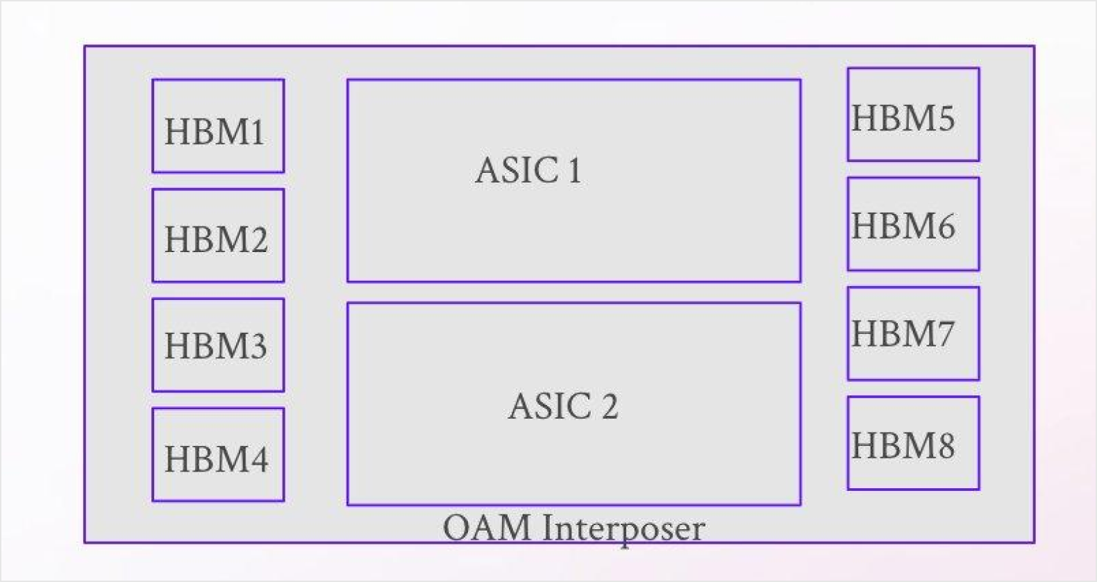
Figure 1 illustrates a representative 2.5D package used in Open Accelerator Module (OAM) systems—the OCP-defined form factor widely deployed for large-scale AI compute. The package integrates two accelerator ASICs and eight HBM stacks on a common interposer. This configuration exposes the core thermal challenge: floorplan decisions—IP block placement, power density distribution, and proximity effects—directly determine HBM junction temperature.
Crucially, this thermal ceiling is set during floorplanning, before full system integration. However, existing workflows do not provide actionable thermal feedback at that stage.
Conventional FEA tools rely on geometry simplification and material homogenization—collapsing BEOL metal layers, micro-bump arrays, and TSV structures into averaged slabs. These approximations suppress the localized hotspot mechanisms that dominate real behavior. At the same time, simulation runtimes remain on the order of days per design point, making iterative exploration impractical.
The result is a fundamental mismatch between problem and tooling: thermal behavior is governed by fine-scale geometry and tight coupling, yet designers are forced to rely on slow, reduced-fidelity models. In practice, this leads to over-conservative guardbands, limited design exploration, and surrendered performance headroom at the system level.
Fig 1: Representative 2.5D package for OAM-based AI accelerator systems — 2 AI accelerator ASICs and 8 HBM stacks co-integrated on a silicon interposer. The constrained floorplan creates heat-trap conditions where IP block placement directly governs thermal coupling into each HBM stack.
2. Physics Intelligence Platform: Manufacturing-Resolution Simulation at Floorplanning Speed
To address the limitations described in Section 1, Vinci developed a system for manufacturing-resolution thermal simulation of 2.5D packages at floorplanning timescales. The system resolves package-level thermal behavior directly on geometry-defined representations, without homogenization or manual meshing.
The method explicitly represents fine-scale structures—including BEOL metal layers (nm–µm scale), micro-bump arrays (~15–20 µm pitch), and TSVs—within a unified package model. Geometry is defined through a structured configuration specifying layer stackups, material assignments, and component placement. Power maps are applied as a separate input, enabling deterministic and reproducible evaluation across large parametric sweeps.
This formulation enables three key properties:
Full-resolution scaling
The system operates directly on geometry-resolved representations of the full package, extending to trillion-scale degrees of freedom. In contrast to conventional FEA workflows, which require coarsening or domain reduction beyond tens of millions of unknowns, all relevant geometric features—including BEOL layers, bump arrays, and TSVs—are preserved at physical dimensions.
Floorplanning-speed runtime
Thermal solutions for a representative 2-ASIC + 16-HBM 2.5D package are obtained in minutes (approximately 6 minutes in our experiments). This enables interactive evaluation of floorplanning decisions, in contrast to conventional workflows where comparable analyses require hours to days.
High-throughput parametric evaluation
The system supports large-scale design-of-experiments (DOE), including variation of power distributions, TIM thickness, and material properties. Thousands of design points can be evaluated in a single overnight run, enabling systematic exploration of thermal design space rather than single-point validation.
Fidelity characteristics
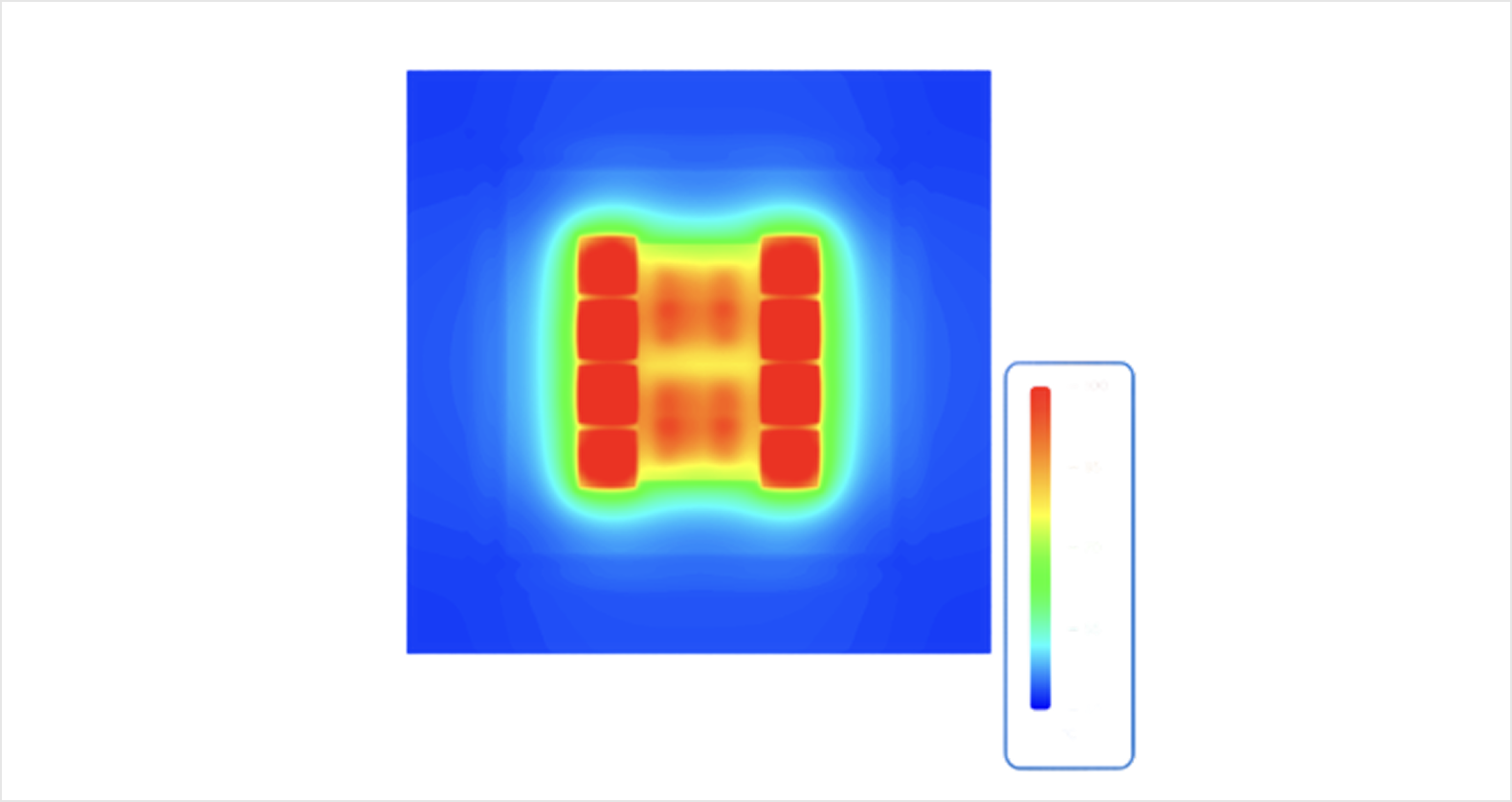
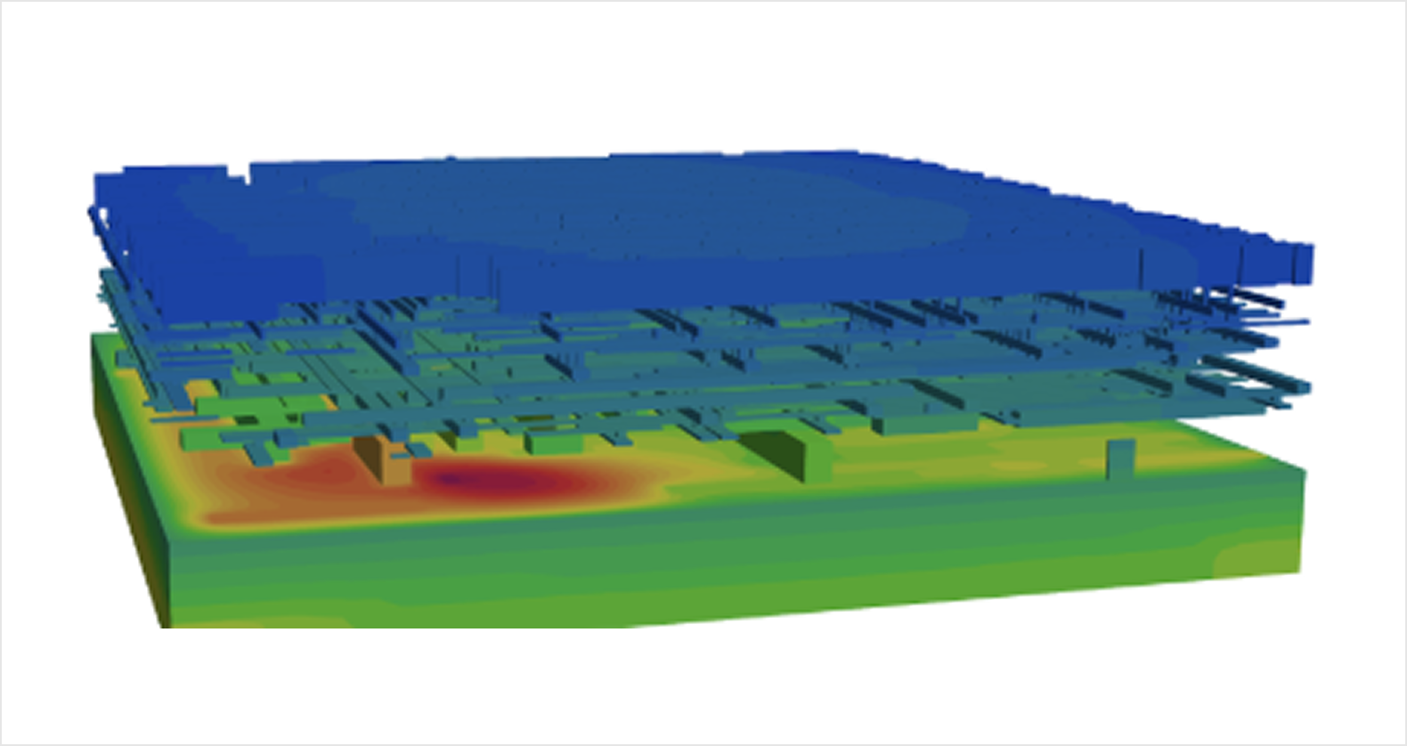
By resolving BEOL metal stacks, micro-bump arrays, and TSVs at their physical dimensions, the method preserves anisotropic thermal resistance and vertical conduction pathways that are suppressed in homogenized models. This enables accurate capture of localized hotspot formation and temperature gradients at bump-pitch granularity, as illustrated in Figures 2 and 3.
Fig 1: Steady-state temperature map across 8 HBM stacks (4 per ASIC) and 2 ASICs at maximum TDP; Tj ≈ 100 °C at HBM.
Fig 2: Explicit representation of the multi-layer stackup including BEOL metal layers, micro-bump arrays, and TSVs at manufacturing resolution — no geometry simplification.
3. Thermal-Aware Floorplanning: Steady-State DOE Results
The methodology is evaluated on a representative 2.5D package comprising two high-power ASICs and sixteen HBM stacks integrated on a silicon interposer and organic substrate. A set of steady-state design-of-experiments (DOE) studies is used to quantify the impact of key floorplanning and packaging variables on junction temperature and thermal coupling.
Four parameter sweeps are considered:
ASIC internal powermap configurations
Thermal interface material (TIM) thickness (25–150 µm)
Bulk TIM conductivity (1–10 W/m·K)
Convective boundary conditions at the package lid (500–3000 W/m²K)
Runtime at full manufacturing resolution
Table 1 summarizes simulation runtime for the full package at manufacturing resolution (~692M degrees of freedom), including explicit representation of BEOL layers and micro-bump structures.
Table 1: Vinci simulation runtime — 692M+ DOF 2.5D package at full manufacturing resolution
Simulation Approach
DOF Count
Wall-clock Time / Case
Vinci (w/o Keff, BEOL+Bump)
692,692,173
92.65 sec
Vinci (w/ Keff, BEOL+Bump)
692,692,173
346 sec
These runtimes enable iterative evaluation of full-package thermal behavior at floorplanning timescales, making large DOE sweeps practical.
Powermap-driven floorplanning
Variation of ASIC internal powermaps shows that IP block placement strongly influences both peak junction temperature and thermal coupling into adjacent HBM stacks. Optimized placement reduces hotspot intensity while limiting lateral heat spreading into memory, expanding the feasible power-density envelope without exceeding HBM temperature constraints.
TIM thickness and conductivity sensitivity
Sweeps across TIM thickness and conductivity quantify the sensitivity of junction temperature to package-level material parameters. The results produce Tj–parameter response curves that directly inform co-design decisions between die implementation and package specification, enabling more precise trade-offs between thermal performance and manufacturability.
Boundary condition sensitivity
Variation in convective boundary conditions at the package lid demonstrates how system-level thermal environment assumptions propagate into junction temperature margin. The results quantify sensitivity to cooling conditions, providing guidance on how conservatively chip-level thermal limits must be specified under uncertainty in deployment environments.
4. Significance for the HotChips Community
For chip architects, SoC designers, and package co-design engineers working on next-generation AI accelerators and HPC systems, this work demonstrates that manufacturing-resolution thermal simulation can be performed at the speed required for floorplanning iteration—not just late-stage verification.
By resolving fine-scale structures while maintaining minute-scale runtimes, the approach enables thermally aware floorplanning decisions to be made early in the design process, where they have the greatest impact on performance, reliability, and system scalability. This directly addresses the growing challenge of thermal coupling in advanced 2.5D and chiplet-based architectures, particularly as systems scale to higher HBM stack counts and finer interconnect geometries.
The results establish a practical pathway for integrating full-fidelity thermal analysis into routine design workflows, replacing over-conservative guardbanding with data-driven optimization. This shift allows architects and package designers to more effectively manage power density, mitigate hotspot formation, and co-optimize die and package design under increasingly constrained thermal budgets.
Keywords:Thermal Floorplanning, 2.5D Integration, HBM, AI Accelerator, Physics Intelligence, TIM Optimization, Powermap DOE, Advanced Packaging, Chiplet Co-Design
Dr. Hardik Kabaria is Founder and Chief Executive Officer of Vinci. His work in computational geometry, physics simulation, and AI underpins the company’s approach to deterministic, solver-accurate systems for engineering and the physical world.
Rahima Mohammed
Semiconductor Technical Advisor
Rahima Mohammed is Semiconductor Technical Advisor at Vinci, where she leads strategy for physics-intelligent modeling and AI-accelerated validation in the semiconductor ecosystem. Her work spans multiphysics modeling across thermal, mechanical, and electrical domains, with a focus on advanced cooling, 3DIC packaging, and benchmarking efforts that inform product direction across component, package, and system levels.
Satish Radhakrishnan
Head of GTM - Semiconductor & Electronics
Satish Radhakrishnan is Head of GTM - Semiconductor & Electronics at Vinci, where he works at the intersection of technical strategy, industry engagement, and adoption across semiconductor and electronics markets. His background in simulation, packaging, and applied physical systems informs a practical, engineering-led perspective on deploying advanced physics-based tools in production workflows.
Vincent Rerolle
Co-Founder & Chief Commercial Officer
Vincent Rerolle is Co-Founder and Chief Commercial Officer at Vinci. He works at the intersection of technical product strategy, industry engagement, and commercialization, helping connect advances in physics-based AI to the practical needs of engineering organizations.
Will Stark
Founding Mechanical Engineer
Will Stark is a founding member of the Vinci team and a mechanical engineer leading core research and platform development across the company’s technical stack. His work helps define the systems and infrastructure behind Vinci’s approach to physics-based AI for engineering.
Sarah Osentoski
Co-Founder & Chief Technology Officer
Dr. Sarah Osentoski is Co-Founder and Chief Technology Officer at Vinci. A leader in machine learning and autonomous systems, she directs Vinci’s technical work at the intersection of AI, physics, and production engineering.
John Bruggeman
Chief Marketing Officer
John Bruggeman is Chief Marketing Officer at Vinci, where he leads the company’s market narrative and strategic positioning. His work focuses on translating complex technical advances into clear category definition, industry relevance, and market adoption.